USD
USD INR
INR
Call Us Now
+91 9106756572
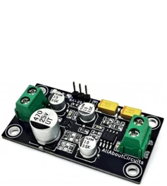
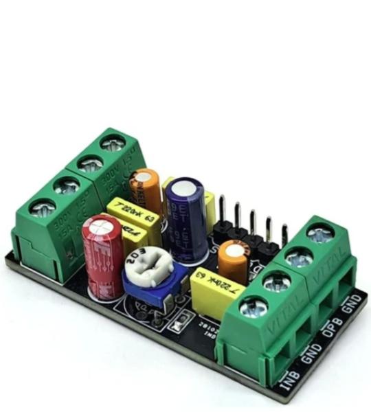
This compact preamplifier module is designed to amplify small signals from high-source-impedance sensors with minimal added noise. It delivers a midband gain of 60 dB and a flat frequency response from approximately 16 Hz to 43 kHz. The clean roll-off at the corner frequencies produces a natural-sounding filter response well suited to audio applications.
This compact preamplifier module is designed to amplify small signals from high-source-impedance sensors with minimal added noise. It delivers a midband gain of 60 dB and a flat frequency response from approximately 16 Hz to 43 kHz. The clean roll-off at the corner frequencies produces a natural-sounding filter response well suited to audio applications.
The board operates from a single 12 V DC supply by default, with an option for dual-supply operation via component substitution. Screw terminals are provided for signal input (CN2) and output (CN3). A 3-pin header (CN1) accepts the power supply connections.
The input signal is AC-coupled through C8 (10 µF) to the gate of U1 (JFE150). Resistor R7 (1 MΩ) sets the DC gate bias.
The JFE150's drain current is proportional to the gate voltage: IDS = gm × VGS. Therefore, it is an effective current-controlled transconductance element. The DC drain bias is set by R5 (4.02 kΩ), which is connected to the +VS rail.
The OPA202 (U2) is configured as a transimpedance amplifier. Its inverting input is driven by the JFET drain current, and feedback resistor R13 (1 MΩ) sets the transimpedance gain.
The non-inverting input is biased by a resistor divider (R2 and R4, both 110 kΩ) that sits at mid-supply (~6 V) in single-supply mode. This VBIAS shifts the OPA202 output DC level to approximately 6 V, keeping it within its linear range on a single rail.
Output isolation resistor R6 (49.9 Ω) improves stability when driving capacitive loads above 1 nF. It can be removed if no capacitive load drive is required.
Power-supply filtering is handled by a ferrite bead (R16, 600 Ω at 100 MHz) in series with the supply rail, supplemented by bulk (C1, 47 µF tantalum) and bypass capacitors (C2, C3, 100 nF each).
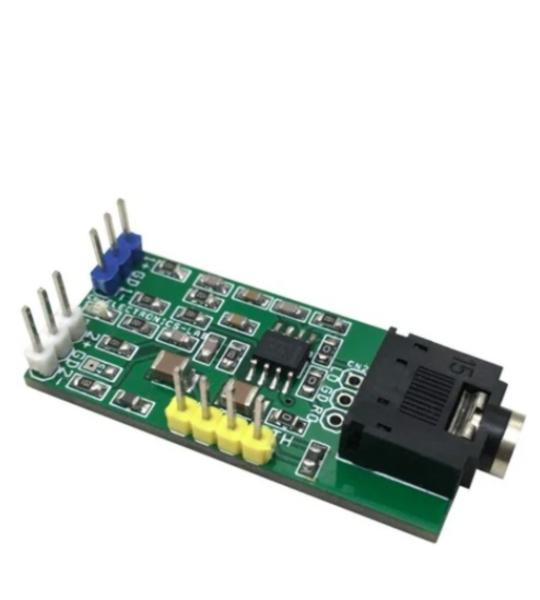
This is a headphone amplifier project for audio digital-to-analog converters (DACs) with differential voltage outputs. This circuit converts the differential voltage output of the DAC to a single-ended, ground-referenced signal and provides the additional current necessary for low-impedance headphones. Project is built using OPA1688 low distortion, high-drive Sound Plus audio amplifier. The circuit tested with dual +/-5V DC supply, and it can drive a load 16 Ohms to 600 Ohms. Headphone amplifier provides an output 50mW into 32 Ohms. Signal for the right channel and left channel input is applied to the amplifier through connectors CN1and CN3, respectively.
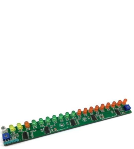
This is an “Audio VU Meter” or “Sound Level Meter”, it is a general-purpose bar-graph Audio VU meter designed for fun projects. All you need is to hook up one wire to the output of the audio amplifier’s speaker pin along with GND and see the magic. The response of the circuit is very fast and it provides beautiful visual representation from audio input signal.
This simple project is an audio limiter based on the NJM2761 chip. It provides effective protection for speakers by limiting the audio signal level. The limit level is adjustable through an external trimmer potentiometer (PR1).
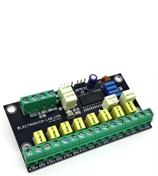
This Audio Processor designed using TDA7440 chip from ST. The chip is a volume tone (bass and treble) balance (Left/Right) processor for quality audio applications in Hi-Fi systems. A selectable input gain is provided. Control of all the functions is accomplished by serial bus I2C. The AC signal setting can be altered by resistor networks and switches combined with operational amplifiers.
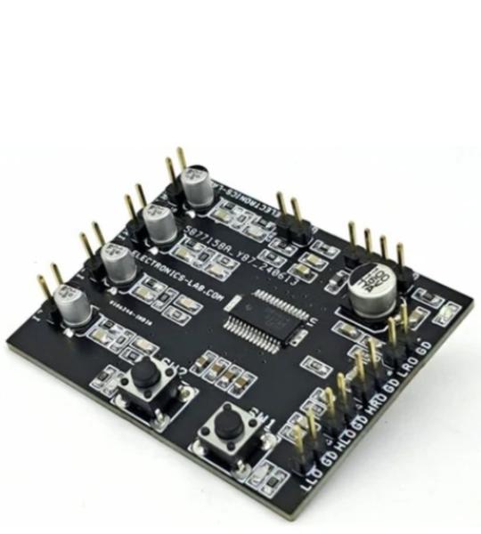
This is a 2Vrms Pop-Free stereo line driver with a stereo headphone driver designed to allow the removal of the output DC-blocking capacitors for reduced component count and cost. The project is based on the DRV604 chip which is ideal for single supply electronics where size and cost are critical design parameters. The project is capable of driving 2Vrms into a 5kΩ load and a clean 40mW into a 32Ω headphone with a single 3.3V supply voltage. Line and headphone outputs have ±8kV IEC ESD protection. The device has built-in shutdown control for pop-free on/off control. The DRV604 does not require a power supply greater than 3.3V to generate its 5.6Vpp output, nor does it require a split rail power supply. The DRV604 integrates its charge pump to generate a negative supply rail that provides a clean, pop-free ground biased 2Vrms output. This project is configured with single-ended header input connectors for analog input, headphones, and line output. The power supply is connected via a four-pin 2.54mm pin header.
Cookie preferences