USD
USD INR
INR
Call Us Now
+91 9106756572
Many high-performance audio digital-to-analog converters (DACs) feature a current output that must be converted into a voltage output for use with audio amplifiers. In premium automotive audio applications, for example, it is critical that the DAC signal-to-noise ratio (SNR) and total harmonic distortion plus noise (THD+N) performance is not compromised by the current-to-voltage (I-V) output stage. The first stage of the circuit converts the current output to a voltage output by providing a virtual ground potential to the OUTP and OUTN nodes of the DAC. The current flowing from the DAC then creates a voltage across the resistor, R4, R18, in the feedback loop. Note that current-output audio DACs have a common mode current that creates an offset to confirm that the DAC is always sourcing current. This common-mode current also results in the output of the first stage always being a negative value. The supplies of the amplifiers of the circuit are not required to be symmetrical. The second stage of the circuit is a differential amplifier that converts the differential voltage of the first stage into a single-ended output voltage. In the third-order, low-pass filter (LPF) circuit, the output level of 2.1 V RMS and 123-dB signal-to noise ratio is achieved. A NE5534 operational amplifier is used for the I/V circuit to obtain the specified performance. Dynamic performance such as the gain bandwidth, settling time, and slew rate of the operational amplifier affects the audio dynamic performance of the I/V section. The current of the PCM1795 device on each of the output pins (IOUTL+, IOUTL–, IOUTR+, IOUTR–) is 4 mA-PP at 0 dB (full-scale).
Many high-performance audio digital-to-analog converters (DACs) feature a current output that must be converted into a voltage output for use with audio amplifiers. In premium automotive audio applications, for example, it is critical that the DAC signal-to-noise ratio (SNR) and total harmonic distortion plus noise (THD+N) performance is not compromised by the current-to-voltage (I-V) output stage. The first stage of the circuit converts the current output to a voltage output by providing a virtual ground potential to the OUTP and OUTN nodes of the DAC. The current flowing from the DAC then creates a voltage across the resistor, R4, R18, in the feedback loop. Note that current-output audio DACs have a common mode current that creates an offset to confirm that the DAC is always sourcing current. This common-mode current also results in the output of the first stage always being a negative value. The supplies of the amplifiers of the circuit are not required to be symmetrical. The second stage of the circuit is a differential amplifier that converts the differential voltage of the first stage into a single-ended output voltage. In the third-order, low-pass filter (LPF) circuit, the output level of 2.1 V RMS and 123-dB signal-to noise ratio is achieved. A NE5534 operational amplifier is used for the I/V circuit to obtain the specified performance. Dynamic performance such as the gain bandwidth, settling time, and slew rate of the operational amplifier affects the audio dynamic performance of the I/V section. The current of the PCM1795 device on each of the output pins (IOUTL+, IOUTL–, IOUTR+, IOUTR–) is 4 mA-PP at 0 dB (full-scale).
This is a headphone amplifier project for audio digital-to-analog converters (DACs) with differential voltage outputs. This circuit converts the differential voltage output of the DAC to a single-ended, ground-referenced signal and provides the additional current necessary for low-impedance headphones. Project is built using OPA1688 low distortion, high-drive Sound Plus audio amplifier. The circuit tested with dual +/-5V DC supply, and it can drive a load 16 Ohms to 600 Ohms. Headphone amplifier provides an output 50mW into 32 Ohms. Signal for the right channel and left channel input is applied to the amplifier through connectors CN1and CN3, respectively.
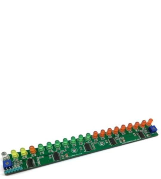
This is an “Audio VU Meter” or “Sound Level Meter”, it is a general-purpose bar-graph Audio VU meter designed for fun projects. All you need is to hook up one wire to the output of the audio amplifier’s speaker pin along with GND and see the magic. The response of the circuit is very fast and it provides beautiful visual representation from audio input signal.
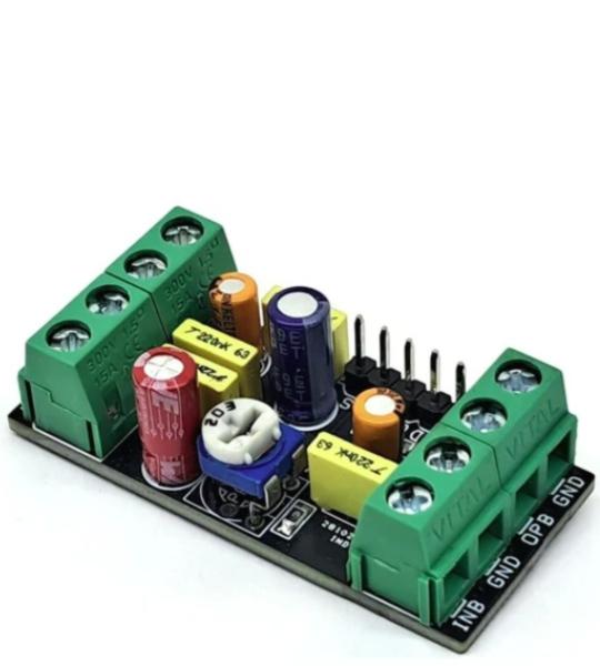
This simple project is an audio limiter based on the NJM2761 chip. It provides effective protection for speakers by limiting the audio signal level. The limit level is adjustable through an external trimmer potentiometer (PR1).
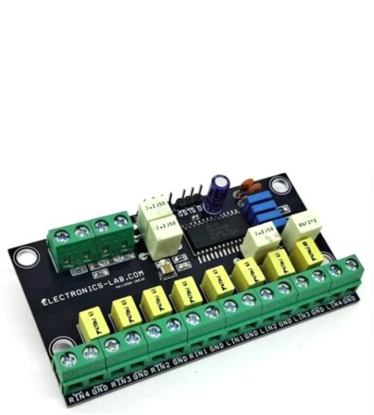
This Audio Processor designed using TDA7440 chip from ST. The chip is a volume tone (bass and treble) balance (Left/Right) processor for quality audio applications in Hi-Fi systems. A selectable input gain is provided. Control of all the functions is accomplished by serial bus I2C. The AC signal setting can be altered by resistor networks and switches combined with operational amplifiers.
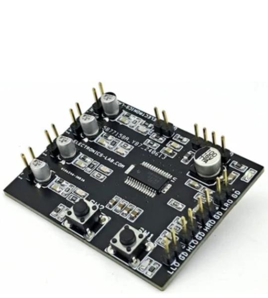
This is a 2Vrms Pop-Free stereo line driver with a stereo headphone driver designed to allow the removal of the output DC-blocking capacitors for reduced component count and cost. The project is based on the DRV604 chip which is ideal for single supply electronics where size and cost are critical design parameters. The project is capable of driving 2Vrms into a 5kΩ load and a clean 40mW into a 32Ω headphone with a single 3.3V supply voltage. Line and headphone outputs have ±8kV IEC ESD protection. The device has built-in shutdown control for pop-free on/off control. The DRV604 does not require a power supply greater than 3.3V to generate its 5.6Vpp output, nor does it require a split rail power supply. The DRV604 integrates its charge pump to generate a negative supply rail that provides a clean, pop-free ground biased 2Vrms output. This project is configured with single-ended header input connectors for analog input, headphones, and line output. The power supply is connected via a four-pin 2.54mm pin header.
Cookie preferences