USD
USD INR
INR
Call Us Now
+91 9106756572
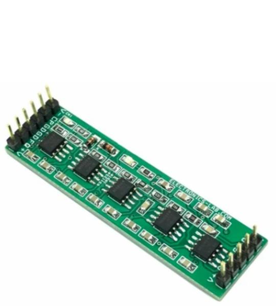
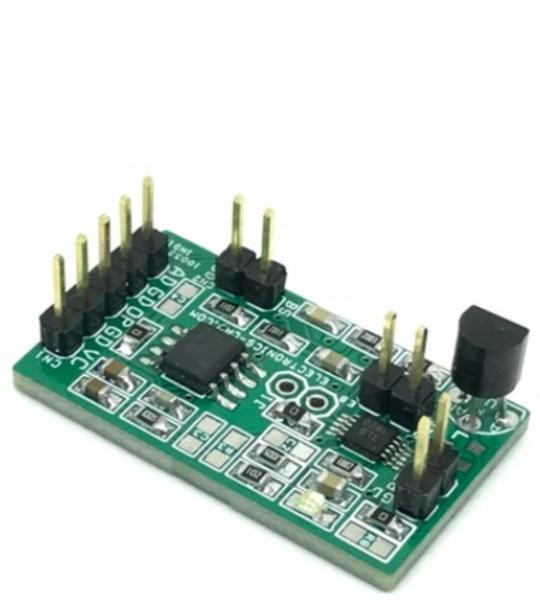
The project presented here is an analog capacitive humidity sensor converter board suitable for various humidity measurement tasks. The circuit comes from Texas Instruments application note (see below). Most conventional capacitive proximity sensors produce a digital signal, but this circuit produces a DC output voltage that is a function of the relative humidity of the environment. The oscillator input for this circuit is a 1Khz sine source (1Vpp) feed to FQ input. The low frequency and sine characteristics keep RFI problems at a minimum. This sensor output converter may prove difficult to construct because of the small capacitances involved, parasitic capacitances in the sensor circuit, and noise pickup. The circuit requires an external 1Khz sinewave with 1Vpp signal and operates with a dual 15V DC supply.
The project presented here is an analog capacitive humidity sensor converter board suitable for various humidity measurement tasks. The circuit comes from Texas Instruments application note (see below). Most conventional capacitive proximity sensors produce a digital signal, but this circuit produces a DC output voltage that is a function of the relative humidity of the environment. The oscillator input for this circuit is a 1Khz sine source (1Vpp) feed to FQ input. The low frequency and sine characteristics keep RFI problems at a minimum. This sensor output converter may prove difficult to construct because of the small capacitances involved, parasitic capacitances in the sensor circuit, and noise pickup. The circuit requires an external 1Khz sinewave with 1Vpp signal and operates with a dual 15V DC supply.
The circuit consists of a complete charge amplifier for the detection of the capacitive sensor’s capacitance change. The charge amplifier is followed by an absolute value circuit which serves as a full-wave rectifier. This part of the circuit converts the varying AC signal from the charge amplifier to a DC voltage, however this DC voltage is unfiltered and contains the carrier frequency ripple.
So the next part of the circuit takes this DC voltage and passes it through a 2-stage, 4-pole low pass filter to remove the ripple. This results in a DC voltage that is a function of the charge amplifier gain. To design the 4th order filter stage, Filter_Pro_v1.3 Tool is used.
The previous charge amplifier circuit produces a stable DC level for a fixed charge amplifier gain. In the diagram below the input sensor capacitance is changed to 3 different values, 160, 180 and 200pF, thus resulting in three different charge amplifier gains and corresponding DC levels.
Further Improvements
The circuit is not overly sensitive and a large DC level is present. Adding gain would help exaggerate the DC charge that results from the capacitance change, but the large DC level would be gained up as well. This would have to be dealt with in a subsequent stage.
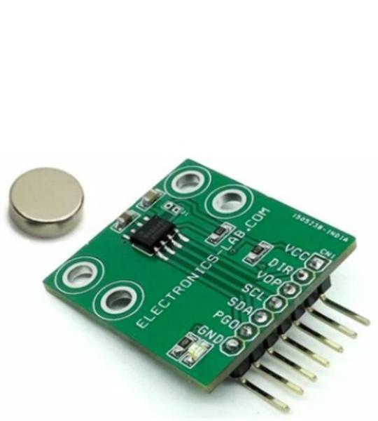
This is an easy-to-program magnetic rotary position sensor with high-resolution 12-bit analog or PWM output. This contactless system measures the absolute angle of a diametric magnetized on-axis magnet. The project is designed for contactless potentiometer applications and its robust design eliminates the influence of any homogenous external stray magnetic fields. The industry-standard I²C interface supports simple user programming of non-volatile parameters without requiring a dedicated programmer. By default, the output represents a range from 0 to 360 degrees. It is also possible to define a smaller range to the output by programming a zero angle (start position) and a maximum angle (stop position). The AS5600 is also equipped with a smart low-power mode feature to automatically reduce power consumption. An input pin (DIR) selects the polarity of the output with regard to rotation direction. If DIR is connected to the ground, the output value increases with clockwise rotation. If DIR is connected to VDD, the output value increases with counterclockwise rotation.
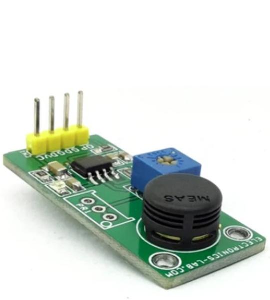
This sensor board provides frequency output as per relative humidity value. The project is based on a unique capacitive cell, this relative humidity sensor is designed for high volume, cost-sensitive applications such as office automation, automotive cabin air control, home appliances, and industrial process control systems. It is also useful in all applications where humidity compensation is needed. The circuit is built using a low-cost NE555 timer as an astable generator, humidity sensor MK1 acts as a variable capacitor and is connected to the TRIG and THRES pin. Pin 7 is used as a short circuit pin for resistor R3. The HS1101LF equivalent capacitor is charged through R2, R3, and PR1 is set the threshold voltage (approximately 0.67Vcc) and discharged through R2 only to the trigger level (approximately 0.33Vcc) since R3 is shortened to the ground by pin 7. Since the charge and discharge of the sensor run through two different resistors, R2 and R3, the duty cycle is determined by the following formulas.
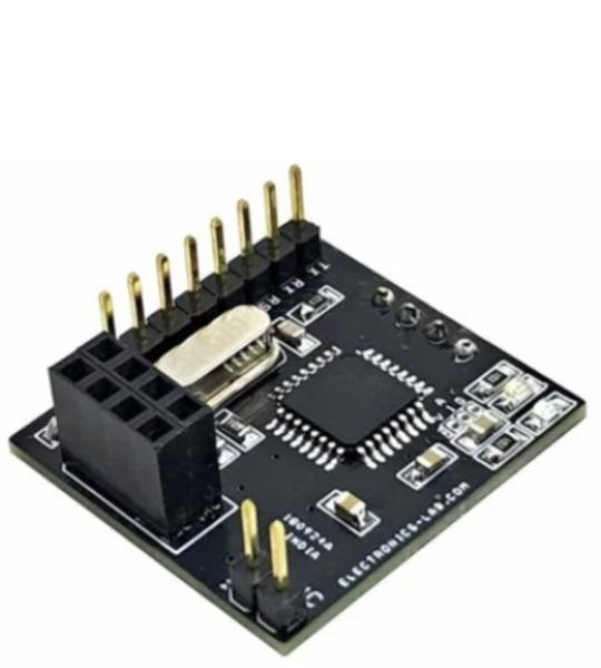
This project is the receiving end of a Wireless Humidity and Temperature monitoring system. The receiver unit is built around an Arduino microcontroller, utilizing the ATMEGA328 chip, which provides a reliable and efficient processing platform. The NRF24L01 transceiver module is used to receive data from the corresponding wireless sensor, while a 0.96-inch I2C OLED display is employed to show the received temperature and humidity values in real time.
This is a simple Proportional, Integral (PI) temperature control amplifier. A complete thermoelectric cooler (TEC) controller can be created using this PI amplifier and OPA569 Power Op-Amp or other output amplifiers such as DRV591, DRV592 and DRV593. Proportional-integrator compensation is simpler to adjust and often provides an adequate thermal transient response to the TEC driver amplifiers. The project consists INA330 chip and OPA2340 OPAMP. The INA330 provides thermistor excitation and generates an output voltage proportional to the difference in resistances applied to the inputs. OPA2340 is used to create the PI closed Loop.
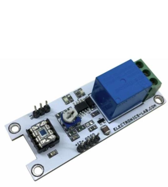
You may have seen many light-sensitive switch circuits based on an LDR sensor. Usually, the sensitivity of the LDR based light sensor is poor. We wanted a very sensitive light switch hence we decided to make a circuit based on a light sensor rather than LDR. After a little research on the internet, we found the OPT101 light sensor chip which includes a photodiode and a transimpedance amplifier in one package. The OPT101 light sensor provides an analog voltage output linearly proportional to light intensity.
Cookie preferences